Why PIC Facet Preparation Matters Before Packaging and Optical Coupling
May 29, 2026, 2:05 p.m.
Why PIC Facet Preparation Matters Before Packaging and Optical Coupling
As photonic integrated circuits, waveguides, and fiber arrays move from research environments toward more scalable applications, the preparation of the optical interface becomes an increasingly important part of the manufacturing process.
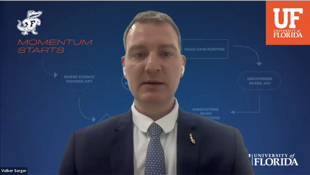
During the Florida Photonics Cluster webinar, “Illuminating Florida’s Growing Semiconductor Industry,” KrellTech’s Tyler Simays, Director of Marketing and Business Development, asked Dr. Volker Sorger about one specific processing challenge: how much of a bottleneck is post-dicing facet preparation before packaging and optical coupling?
The question focused on a practical step that can have a major effect on device performance. After a photonic chip, waveguide, or related component is diced, the resulting edge or facet may need additional preparation before it can be efficiently coupled to fiber arrays, optical assemblies, or other system-level components.
The Importance of the Optical Interface
In photonics, the edge of a device is not just a physical boundary. It is often the point where light enters or exits the component. That makes the quality of the facet especially important.
A poorly prepared interface can contribute to insertion loss, unwanted reflection, coupling inefficiency, and overall performance variability. For research teams, this can make it harder to evaluate designs accurately. For manufacturers, it can create challenges with repeatability, yield, and process control.
As devices become more complex and move toward higher-volume applications, small processing details can become larger production bottlenecks. Facet quality, alignment, geometry, and inspection all play a role in whether an optical connection can be made efficiently and consistently.
From R&D to Scalable Photonics Manufacturing
Many photonic components begin in research and development environments where processes are often customized, manual, or built around a specific experiment. As those devices move closer to production, the same process steps need to become more repeatable, measurable, and scalable.
This is where post-dicing preparation can become a critical step. The challenge is not only to polish or shape a surface, but to do so in a controlled way that supports the customer’s required geometry, surface finish, and coupling performance.
For PICs, waveguides, fiber arrays, and related photonic components, preparation before packaging and optical coupling can influence the success of the next step in the process. If the optical interface is not ready, downstream packaging and testing may be affected.
How KrellTech Supports Photonic Component Processing
At KrellTech, we design and manufacture precision polishing, shaping, and inspection systems for photonic components. Our equipment helps customers develop baseline polishing processes, refine component geometries, inspect results, and troubleshoot challenging applications.
These systems are used across a range of photonics applications, including bare fibers, connectors, ferrules, fiber arrays, waveguides, PICs, and other custom optical components. The goal is to give engineers, researchers, and manufacturers more control over the processing steps that directly affect optical performance.
Conversations with industry leaders, universities, research teams, and photonics organizations help us better understand where the industry is heading. They also help us continue adapting our systems to support real processing needs as photonics applications grow across communications, sensing, AI, semiconductor packaging, and advanced manufacturing.
Continuing the Conversation
The Florida Photonics Cluster webinar highlighted the growing connection between photonics and the broader semiconductor industry. As these ecosystems continue to develop, practical manufacturing steps such as facet preparation, polishing, shaping, and inspection will remain important parts of the conversation.
For KrellTech, engaging in these discussions is part of understanding how our equipment can support the next generation of photonic devices, from university research labs to emerging production environments.
Watch the video clip to hear the discussion on post-dicing facet preparation and its role in packaging and optical coupling.
Watch here: https://krelltech.com/videos/watch/pic-facet-preparation-packaging-coupling/